


RF IPD
Negotiable Min Order Quantity Unit
- Required Quantity
-
- Place of Origin
- Payment Terms
- Negotiable
- Production method
- Negotiable
- Shipping / Lead Time
- Negotiable / Negotiable
- Keyword
- Category
- Other Computer Accessories
Apply a video call to the Supplier
![]()
H&S HighTech Corp.
- Country / Year Established
-
 South Korea
/
1998
South Korea
/
1998
- Business type
- Manufacturer
- Verified Certificate
-
16


| Product name | RF IPD | Certification | - |
|---|---|---|---|
| Category | Other Computer Accessories | Ingredients | - |
| Keyword | - | Unit Size | - |
| Brand name | - | Unit Weigh | - |
| origin | Stock | - | |
| Supply type | - | HS code | - |
Product Information
Descriptions
Telephus' TBL24C201 is a balun for Wireless LAN, Bluetooth applications which is supplied as wafer level CSP. The balun has low insertion loss in pass band and low amplitude and phase difference. It is composed of 10 um Cu-plated inductors and Metal-Insulator-Metal capacitors, which are fabricated on Si Smart Substrate with 25 um thick oxide layer by Telephus' RFIPD (Integrated Passive Device) process. The bump size and pitch of the balun are selected such that the device can be placed directly on PCB using the conventional surface mounting techniques. The solder bump contacts are a 63Sn/37Pb alloy or lead free and are nominally 0.30 mm in diameter.
Features
- Passive integration on Si Smart Substrate
- Low insertion loss in pass band
- Low amplitude and phase difference
- Operating temperature: -40 to +85 °C
- Storage temperature: -40 to +85 °C
- Small size: 1.2 mm ?1.85 mm
- Eutectic Sn/Pb or lead-free solder bump
- Ultra small footprint, 0.65 mm pitch
- Directly attachable on PCB
- Packaged in tape and reel
Electrical Specifications
|
Specification
|
Minimum
|
Typical
|
Maximum
|
Note
|
|
Frequency Range (MHz)
|
2400
|
-
|
2500
|
-
|
|
Insertion Loss (dB)
|
-
|
0.5
|
-
|
-
|
|
Bandwidth VSWR (in, out)
|
-
|
1.5
|
-
|
-
|
|
Unbal./Bal. Impedance (ohm)
|
-
|
50/100
|
-
|
-
|
|
Phase Difference (degree)
|
-
|
180± 3
|
-
|
-
|
|
Amplitude Difference (dB)
|
-
|
0.3
|
-
|
-
|
Typical Characteristics
 |
Typical Solder Reflow Thermal Profile (No Clean Flux)
 |
Physical Dimensions
 |
Notes:
- 63Sn/37Pb eutectic bump
- Recommend non-solder mask defined landing pad.
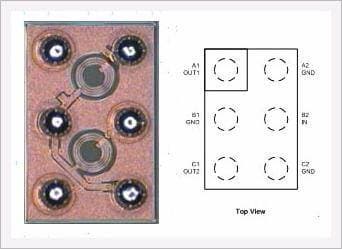
- Pin A1 is established by lower right corner with respect to text orientation. Remaining pins are numbered counter clockwise.
Land pattern Recommendation
Two types of land patterns are used for surface mount packages,
- Non-solder mask defined (NSMD)
- Solder mask defined (SMD)
 |
Notes:
- NSMD configuration is preferred due to its tighter control on copper etch process and a reduction in the stress concentration points on the PCB side compared to SMD configuration.
- A copper layer thickness than 1 oz is recommended to achieve higher stand-off. A 1 oz. (30 micron) or greater copper thickness results in a lowering of the effective stand-off, which may compromise solder joint reliability.
- For the NSMD pad geometry, the trace width at the connection to the land pad should not exceed 2/3 of the pad diameter. The recommended pad geometry is shown in Table1.
|
Pad Definition
|
Large Bump Size (0.3mm Diameter)
|
|
|
Copper Pad
|
Solder Mask Opening
|
|
|
NSMD
|
0.275± 0.025mm
|
0.375± 0.025mm
|
|
SMD
|
0.375± 0.025mm
|
0.275± 0.025mm
|
TABLE 1. Recommended PCB Pad Geometry
B2B Trade
| Price (FOB) | Negotiable | transportation | - |
|---|---|---|---|
| MOQ | Negotiable | Leadtime | Negotiable |
| Payment Options | Negotiable | Shipping time | Negotiable |
![]()
- President
- Ilkwon Dong
- Address
- 25-11, Jang-dong, Yuseong-gu, Daejeon, 305-343, Korea
- Product Category
- Other Telecommunications Equipment
- Year Established
- 1998
- No. of Total Employees
- 1-50
- Company introduction
-
Telephus Inc. is a venture corporation that develops, manufactures, and markets wireless telecommunication components with its own design capability and innovative smart substrate technology. The value of Telephus products is its breakthrough, patented manufacturing technology for smart silicon substrates, which creates demonstrable customer benefits in term of cost, function, and product reliability.
For instance, with a new concept of RF IC design (called "TR-Array") spun off from smart substrate technology, Telephus has received an award from ECTC, US, 2000 (sponsored by Motorola). Smart Substrate Technology provides outstanding cost benefit by integrating numerous passive components of GaAs (or SiGe) RF IC into a silicon substrate without any sacrifice of electrical property.
In addition, for diversified product lines in the semiconductor component industry, Telephus has developed an innovative ACF (Antistrophic Conductive Film: Advanced Electronic Package Material) showing significant improvement of T/C (Thermal Cycle) reliability of flip chip on organic substrates with lower CTE and higher modulus of NCF layer.
- Main Markets
-
 China
China
 Hong Kong(China)
 Japan
Japan
 Malaysia
 Philippines
- Main Product


Related Products

Bluetooth Dongle BU-4096

Perfect Music Server Player – sMS-1000

DUO digital presentation pen

PENNA ( retro wireless bluetooth keyboard)

PASSPORT READER
