


CDMA 1X 450/800/1900M Wireless Engine
Negotiable Min Order Quantity Unit
- Required Quantity
-
- Place of Origin
- Payment Terms
- Negotiable
- Production method
- Negotiable
- Shipping / Lead Time
- Negotiable / Negotiable
- Keyword
- Category
- Mobile Phones
Apply a video call to the Supplier
![]()
G-Mode Co., Ltd.
- Country / Year Established
-
 South Korea
/
South Korea
/
- Business type
- Others
- Verified Certificate
-
16


| Product name | CDMA 1X 450/800/1900M Wireless Engine | Certification | - |
|---|---|---|---|
| Category | Mobile Phones | Ingredients | - |
| Keyword | - | Unit Size | - |
| Brand name | - | Unit Weigh | - |
| origin | Stock | - | |
| Supply type | - | HS code | - |
Product Information
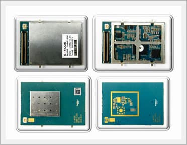
CDMA 1X 450/800/1900M Wireless Engine
|
Top View(CDMA 800/1900MHz)
|
 |
|
Bottom View(CDMA 450MHz)
|
 |
Model Name
|
Frequency Band
|
Model Name
|
Dimension
|
Weight
|
|
CDMA 1x 410/450M
|
GMM-F300
|
45x30x4.8mm
|
8g
|
|
CDMA 1x 800M
|
GMM-C300
|
45x30x3.2mm
|
7g
|
|
CDMA 1x 1900M
|
GMM-P300
|
45x30x3.2mm
|
7g
|
|
CDMA 1x 800/1900M
|
GMM-S300
|
45x30x3.2mm
|
7g
|
Technical Specifications
|
Data Services
|
CDMA 1x RTT (IS-2000) Forward and reverse link speeds: up to 153.6Kbps * Limit to Network conditionsa |
|
Main Chip-set
|
Qualcomm QSC1110 One chip solution Memory: 128M Flash/32 SRAM |
|
Frequency Bands
|
CDMA 410MHz (Band Class 5) ( L-Block) CDMA 450MHz (Band Class 5) (A, C-Block) CDMA 800MHz (Band Class 0) CDMA 1900MHz (Band Class 1) |
|
General Features
|
Voice/Data service MT/MO Test and PDU modes(SMS) Analog (differential/single) audio support Serial UART interface R-UIM support USB interface User applicable GPIOs Power on/off switch Compact, lightweight form factor Complete shielding |
|
AT command
|
G-mode proprietary AT commands Qualcomm proprietary AT commands Operator proprietary AT commands |
|
Environments
|
Operating Temperature: -20°C to 50°C Storage Temperature : -30°C to 70°C Humidity: 95% (non-condensing) |
|
Standards
|
IS-2000 (CDMA 1x RTT) IS-95 A/B IS-707-A Data service IS-683A Service Provisioning IS-707 AT command |
|
Electricals
|
Maximum RF Output Power:+23dBm Receiver Sensitivity : under -106dBm (FER=5%) Nominal Operating Voltage : +3.4VDC ~ +4.2VDC Power Consumption : Maximum: under 600mA : Sleep mode: under 1mA |
|
Mechanicals
|
Antenna connector : SWD type (Primary & Secondary) Mounting: Shield CAN Wing Solder type System interface: 80pin connector |
[80PIN Connector PIN Description]
|
PIN
|
Signal
|
PAD Type
|
Function
|
Type
QSC1110 |
|
1
|
VBATT
|
npPDpuk
|
Main power supply
|
power
|
|
2
|
VBATT
|
-
|
Main power supply
|
power
|
|
3
|
VBATT
|
-
|
Main power supply
|
power
|
|
4
|
VBATT
|
-
|
Main power supply
|
power
|
|
5
|
GND
|
-
|
Ground
|
power
|
|
6
|
GND
|
-
|
Ground
|
power
|
|
7
|
GND
|
-
|
Ground
|
power
|
|
8
|
SPEAKER_OP
|
AO
|
Speaker driver (+) output.
|
Speaker
|
|
9
|
HP_OUT_R_N
|
AO
|
Hand-free ear output, phase +
|
Audio
|
|
10
|
HP_OUT_L_P
|
AO
|
Hand-free ear output, phase -
|
Audio
|
|
11
|
EAROP
|
AO
|
Earphone amplifier output (+).
|
Audio
|
|
12
|
EAROP
|
AO
|
Earphone amplifier output (-).
|
Audio
|
|
13
|
MIC2P
|
AI
|
Microphone #2 input (+)
|
Audio
|
|
14
|
MIC2N
|
AI
|
Microphone #2 input (-).
|
|
|
15
|
MIC1P
|
AI
|
Microphone #1 input (+).
|
Audio
|
|
16
|
MIC1N
|
AI
|
Microphone #1 input (-).
|
Audio
|
|
17
|
GPIO24
|
BS
|
Configurable I/O ( LCD_SCL)
|
LCD
|
|
18
|
VREG-USIM
|
AO
|
External SIM signal -Power supply for the SIM
|
1.8/2.85V
|
|
19
|
UIM_RESET
|
DO
|
RUIM reset/(GPIO_14)
|
1.8/2.85V
|
|
20
|
UIM_DATA
|
BBS-
npPDpuk |
RUIM_DATA/(GPIO_15)
|
1.8/2.85V
|
|
21
|
DNI
|
|||
|
22
|
UIM_CLK
|
DOBS-npPDpuk
|
RUIM clock/(GPIO_12)
|
1.8/2.85V
|
|
23
|
SDCC_DATA2
|
B
|
SDIO data bit 2 / (GPIO_27)
|
2.85V
|
|
24
|
SDCC_DATA0
|
B
|
SDIO data bit 0 / (GPIO_25)
|
2.85V
|
|
25
|
UART1_TX_DATA
|
DO
|
UART transmit data to BT device / (GPIO_19)
|
1.8V
|
|
26
|
UART1_RX_DATA
|
DI
|
UART receive data from BT device / (GPIO_18)
|
1.8V
|
|
27
|
DNI
|
|||
|
28
|
UART1_CTS_N
|
DI
|
Low-speed UART clear to send signal / (GPIO_17)
|
1.8V
|
|
29
|
DNI
|
|||
|
30
|
Speaker_ON
|
AO |
Speaker driver (-) output
|
Speaker
|
|
31
|
UART1_RFR_N
|
DO
|
Low-speed UART ready for receive signal / (GPIO_16)signal
|
1.8V
|
|
32
|
VREG_MSME1
|
AO
|
provided by VREG_MSME1 +1.8V
|
1.8V
|
|
33
|
GPIO26
|
BS
|
Configurable I/O (LCD-SDA)
|
LCD
|
|
34
|
GPIO28
|
BS
|
Configurable I/O (LCD_RS)
|
LCD
|
|
35
|
DNI
|
|||
|
36
|
LCD_DRV_N
|
AO
|
This pin is a dedicated high current driver output pin
|
LCD
|
|
37
|
HKADC0
|
AI
|
Analog multiplexer input channels to the on-chip house-Keeping analog-to-digital converter
|
A/D
|
|
38
|
HKADC1
|
AI
|
A/D
|
|
|
39
|
RTCK
|
DO
|
JTAG return clock
|
1.8V
|
|
40
|
TDO
|
Z
|
JTAG test data output
|
1.8V
|
|
41
|
TDI
|
DI-PU
|
JTAG test data input
|
1.8V
|
|
42
|
TMS
|
DI-PU
|
JTAG test mode select
|
1.8V
|
|
43
|
TCK
|
DI-PU
|
JTAG clock input
|
1.8V
|
|
44
|
TRST_N
|
DI-PD
|
JTAG reset
|
1.8V
|
|
45
|
GPIO29
|
BS
|
Configurable I/O (LCD_RST_N)
|
LCD
|
|
46
|
GND
|
-
|
Ground
|
Power
|
|
47
|
GPIO31
|
BS
|
Configurable I/O (LCD_CS_N)
|
LCD
|
|
48
|
USB_VBUS
|
AI
|
Input supply voltage for on-chip
USBtransceiver; sourced From external USB host. |
4.4V~5.5V
|
|
49
|
PS_HOLD
|
DI
|
Baseband circuits drive this input high to keep power on, low to shut down.
|
PS_HOLD
|
|
50
|
VREG_MSME2
(+2.85V) |
AO
|
Linear regulator output that powers peripheral functions and internal circuits requiring a higher supply voltage thanprovided byVREG_MSME2
|
2.85V
|
|
51
|
Charge
|
AI
|
Charger input
|
Power
|
|
52
|
Charge
|
AI
|
Charger input
|
Power
|
|
53
|
KPD_PWR_N
|
AI
|
Input command for switching power ON or OFFConnect to the keypad power button. Thissignal is pull up internally to dVDD. When the QSC device is off,pulling this pin lowinitiatesa power up and generatesan interrupt.
|
Pull up to VBATT
|
|
54
|
PON_RESET_N
|
DO
|
Connected internally to RESIN_N
|
Reset
|
|
55
|
DNI
|
|||
|
56
|
KYPD_MEMO
|
DO
|
Keypad driver / (GPIO_4)
|
1.8V
|
|
57
|
KYPD_17
|
DO
|
Keypad driver (17) / (GPIO_3)
|
1.8V
|
|
58
|
KYPD_15
|
DO
|
Keypad driver (15) / (GPIO_2)
|
1.8V
|
|
59
|
KYPD_11
|
DO
|
Keypad driver (11) / (GPIO_1)
|
1.8V
|
|
60
|
KYPD_9
|
DO
|
Keypad driver (9) / (GPIO_0)
|
1.8V
|
|
61
|
KEYSENSE4_N
|
DI
|
Bit 4 for sensing key press on pad matrix / (GPIO_5)matrix
|
1.8V
|
|
62
|
KEYSENSE3_N
|
DI
|
Bit 3 for sensing key press on pad matrix / (GPIO_6)
|
1.8V
|
|
63
|
KEYSENSE2_N
|
DI
|
Bit 2 for sensing key press on pad matrix / (GPIO_7)
|
1.8V
|
|
64
|
KEYSENSE1_N
|
DI
|
Bit 1 for sensing key press on pad matrix / (GPIO_8)
|
1.8V
|
|
65
|
KEYSENSE0_N
|
DI
|
Bit 0 for sensing key press on pad matrix / (GPIO_9)
|
1.8V
|
|
66
|
AUX_PCM_SYNC
|
DO
|
Auxiliary PCM interface sync / (GPIO_21)
|
1.8V
|
|
67
|
AUX_PCM_DIN
|
DI
|
Bluetooth PCM I/F data in (if QSC master) / (GPIO_22)
|
1.8V
|
|
68
|
AUX_PCM_DOUT
|
DO
|
Bluetooth PCM I/F data out (if QSC master) / (GPIO_23)
|
1.8V
|
|
69
|
AUX_PCM_CLK
|
DO
|
Clock for Bluetooth PCM interface / (GPIO_20)
|
1.8V
|
|
70
|
I2C_SCL
|
B
|
I2C clock / (GPIO_40)
|
1.8V
|
|
71
|
I2C_SDA
|
B
|
I2C data / (GPIO_39)
|
1.8V
|
|
72
|
(GPIO_41)
|
BS
|
Configurable I/O
|
1.8V
|
|
73
|
(GPIO_42)
|
BS
|
Configurable I/O
|
1.8V
|
|
74
|
(GPIO_43)
|
BS
|
Configurable I/O
|
1.8V
|
|
75
|
(GPIO_44)
|
BS
|
Configurable I/O
|
1.8V
|
|
76
|
(GPIO_48)
|
BS
|
Configurable I/O
|
1.8V/2.6V
|
|
77
|
(GPIO_49)
|
BS
|
Configurable I/O
|
1.8V/2.6V
|
|
78
|
(GPIO_50)
|
BS
|
Configurable I/O
|
1.8V/2.6V
|
|
79
|
USB_DP
|
AI/AO
|
USB differential data, (+) side
|
USB
|
|
80
|
USB_DM
|
AI/AO
|
USB differential data, (-) side
|
USB
|
B2B Trade
| Price (FOB) | Negotiable | transportation | - |
|---|---|---|---|
| MOQ | Negotiable | Leadtime | Negotiable |
| Payment Options | Negotiable | Shipping time | Negotiable |
- President
- Jae Myung, Kim
- Address
- Rm805, Kranz Techno, 5442-1, Sangdaewon 1-dong, Seongnam Si Jungwon-gu, GYEONGGI-DO, 462-729, KOREA
- Product Category
- Cordless Telephones,Mobile Phones
- No. of Total Employees
- 1-50
- Company introduction
-
INTRO HEALTH has been established since October 2006 after renaming of the mother company SOOSAN GIC established in 2002.
INTRO HEALTH has two main products. One is the medical device section includes with Locking Pigtail Drainage Catheters (Multipurpose, Nephrostomy and PTBD)and 'RECOPINE' KYPHOPLASTY KIT used for restoration of spine fractures,which has been already proven its quality globally. We can supply customized design with bulk, non-sterile package in oem base as well.
- Main Product


