


RF GaN Epi Wafer HEMT Structure On SiC Manufacturer
RF GaN Epi Wafer HEMT Structure On SiC Manufacturer
Negotiable Min Order Quantity Unit
- Required Quantity
-
- Place of Origin
- China
- Payment Terms
- T/T
- Production method
- Available
- Shipping / Lead Time
- Negotiable / Negotiable
- Category
- Semiconductors
Apply a video call to the Supplier
![]()
Suzhou Hengmairui Materials Technology Co.,Ltd.
 China
China
- Verified Certificate
-
9


| Product name | RF GaN Epi Wafer HEMT Structure On SiC Manufacturer | Certification | - |
|---|---|---|---|
| Category | Semiconductors | Material | - |
| Keyword | gan epi wafer on sic rf hemt manufacturer , algan/gan on sic hemt epi wafer manufacturer | Unit Size | - |
| Brand name | - | Unit Weigh | - |
| origin | China | Stock | 15 |
| Supply type | Available | HS code | - |
Product Information
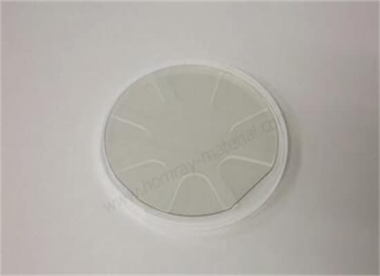
RF GaN Epi Wafer HEMT Structure On SiC Manufacturer
HMT supply 4 inch GaN HEMT wafer on SiC with favourable price on the market for domestic and foreign customers. GaN Epi Wafer is a high-quality wafer used for the fabrication of RF HEMT devices. It consists of a SiC substrate, a thin SiN layer, and a GaN buffer layer. The SiN layer is essential for providing excellent surface passivation and improving device performance. The AlGaN/GaN layers on top of the GaN buffer layer form the active region of the device, allowing for high-frequency operation and high-power handling capabilities.The Al content in the AlGaN layer can be customized according to the specific needs of the device, ranging from 15% to 30%. This flexibility allows for the optimization of device performance for various applications. The bow of the wafer is also strictly controlled to be ≤±50um, ensuring uniformity and consistency in device fabrication.
Moreover, the use of SiC as the substrate offers excellent thermal conductivity and high breakdown voltage, making it an ideal choice for high-power and high-temperature applications. The GaN buffer layer, with a thickness of 2-3nm, serves as a transition layer between the SiC substrate and the active device layers, providing strain relief and improving the crystal quality of the device.
B2B Trade
| Price (FOB) | Negotiable | transportation | Air Transportation |
|---|---|---|---|
| MOQ | Negotiable | Leadtime | Negotiable |
| Payment Options | T/T | Shipping time | Negotiable |
![]()
- President
- Cory
- Address
- LiSheng Industrial Building,60 Suli Road
- Product Category
- Semiconductors
- Year Established
- 2009
- No. of Total Employees
- 51-100
- Company introduction
-
Homray Material Technology(HMT)was established in 2009, is a leading manufacturer and supplier of Gallium Nitride(GaN) Substrate Wafer(GaN-On-Sapphire Template, Free-standing GaN Wafer), GaN Epi Wafer (GaN-On-Si Epi Wafer, GaN-On-Sapphire Epi Wafer, GaN-On-SiC Epi Wafer), and Silicon Carbide(SiC) Substrate Wafer, SiC Epi Wafer, Silicon Test Wafer etc. It is widely acknowledged that compound Semiconductor (GaN, SiC) with its superior property like wide-bandgap, is expected to the most promising material choice for next generation device. GaN device/module and SiC device/module can achieve low losses and fast switching/oscillation simultaneously because of its high critical electrical field. Homray Material Technology is committed to developing high quality GaN Wafer and SiC Wafer for HEMT RF, power electronics and opto-electronics applications. As the leading Substrate Wafer and Epi Wafer manufacturer and supplier in the semiconductor industry, our dealers and partners are mainly distributed in Europe, USA, Southeast Asia, and South America, our sales value exceeded 65 Million US dollars in 2020. Excellent products quality and professional service won the trust and support from our customers in the world as well as our share of market.
- Main Product


